
During my doctoral research in Green Electronics at TU Munich, I spent hundreds of hours in cleanrooms working on microfabrication protocols. That experience left a lasting impression on how I view hardware development. As electrical engineers, we often marvel at sub-micron precision and nanometer-scale architecture, but the physical reality behind that performance involves aggressive chemical processing. Hydrofluoric acid, ammonium fluoride, and high-GWP fluorinated etching gases are fundamental to defining the conductive pathways on silicon wafers, yet their environmental cost cannot be ignored.
When I cycle to the lab or experiment with reclaimed materials in my workshop, I am constantly reminded of the natural systems we must protect. Every high-performance chip powering our smart gadgets, low-power microcontrollers, and renewable energy infrastructure relies on chemical processing steps that produce volatile organic compounds, hazardous liquid waste, and toxic effluents.
The engineering community must confront this contradiction directly. True technological innovation cannot rely on linear, destructive chemical lifecycles. We have to understand the chemistry behind wafer etching not merely to optimize yields, but to take accountability for worker safety, local watershed preservation, and atmospheric emissions right from the initial design phase.
Etching chemicals are vital in semiconductor manufacturing, but they can also contribute to significant pollution. Their use poses health risks, including respiratory issues and skin irritations, while also contaminating air and water systems. To address these challenges, there are strict regulations and innovative practices aimed at minimizing waste and reducing environmental impact. Understanding these complexities is essential for anyone involved in chip production. Learn more about the sustainable trends transforming this industry.
KEY TAKEAWAYS
- Etching chemicals like hydrofluoric acid are crucial in semiconductor manufacturing but can release harmful VOCs, contributing to air and water pollution.
- Improper disposal of spent etching solutions poses significant risks of soil contamination, necessitating advanced waste management strategies.
- Exposure to etching chemicals can lead to serious health issues, including respiratory problems and skin irritations, highlighting the need for safety protocols.
- Regulatory frameworks enforce limits on etching chemicals and mandate worker safety training to minimize health and environmental risks.
- Adopting eco-friendly alternatives and recycling practices can significantly reduce waste and environmental impact in semiconductor chip production.
WHAT YOU NEED TO KNOW ABOUT ETCHING CHEMICALS IN SEMICONDUCTOR MANUFACTURING
The semiconductor industry has a problem. Demand is booming for silicon chips, which are embedded in everything from smartphones and televisions to wind turbines, but it comes at a big cost: a huge carbon footprint.
When you plunge into semiconductor manufacturing, understanding etching chemicals is essential for achieving precision in microfabrication. These chemicals play a pivotal role in etching processes, allowing for the selective removal of material from silicon wafers.
Familiarize yourself with various etching agents—such as hydrofluoric acid and ammonium fluoride—as each has unique properties that influence etching rates and outcomes.
Moreover, prioritize chemical safety in your operations. Proper handling, storage, and disposal of etching chemicals are vital to protect both personnel and the environment.
Implementing stringent safety protocols helps mitigate risks associated with exposure and contamination.
Investing in the right equipment and training can enhance your etching capabilities while ensuring compliance with safety regulations.
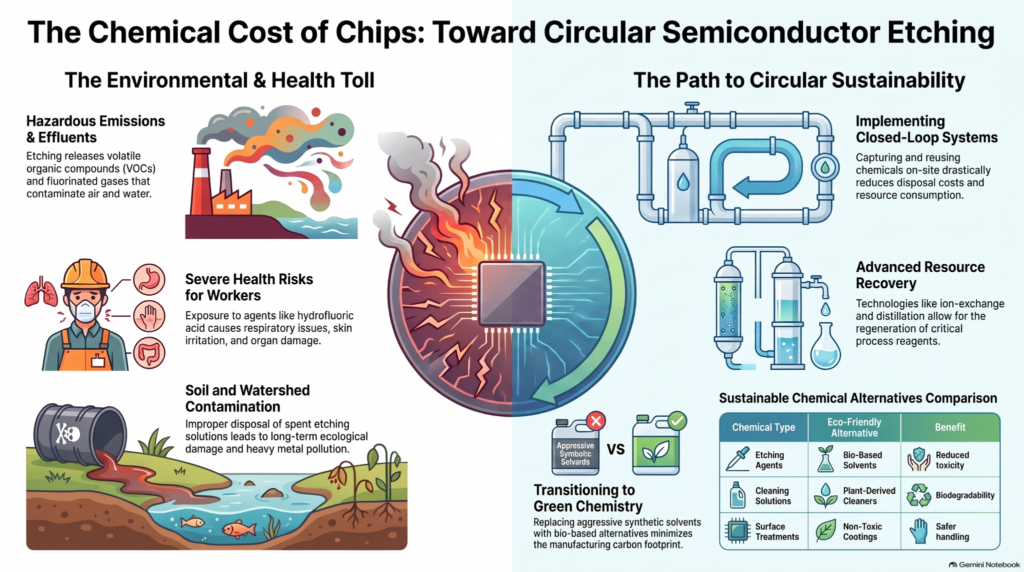
How Etching Chemicals Contribute to Pollution
Etching chemicals, while essential for precision in semiconductor manufacturing, can pose considerable pollution risks if not managed properly. During etching processes, these chemicals interact with various materials, leading to byproducts that may be harmful to the environment. If released into the atmosphere or water systems, volatile organic compounds (VOCs) and other hazardous substances can contribute to air and water pollution, impacting local ecosystems.
Moreover, improper disposal of spent etching solutions can result in soil contamination, further exacerbating environmental challenges, similar to concerns associated with cobalt mining environmental chemical impact. The chemical interactions that occur during etching not only affect the efficiency of semiconductor production but also raise concerns about long-term ecological impacts.
To mitigate these risks, it’s vital to implement advanced waste management strategies and invest in innovative containment technologies.
Health Risks and Pollution From Etching Chemicals in Chip Production
Numerous health risks arise from exposure to etching chemicals used in chip production, requiring strict safety protocols. These chemicals, including hydrofluoric acid and peracetic acid, can lead to severe respiratory issues, skin irritations, and long-term organ damage.
When inhaled or absorbed, they pose significant health impacts, affecting not only workers but also surrounding communities.
The release of these substances into the environment raises additional environmental concerns. Contaminated wastewater and airborne particles can harm local ecosystems, affecting air and water quality.
Workers must be equipped with appropriate protective gear, and facilities should implement advanced ventilation systems to mitigate exposure risks.
As the semiconductor industry continues to innovate, prioritizing safety and environmental responsibility becomes essential.
Understanding the implications of etching chemicals fosters a safer workplace and promotes sustainable practices, ultimately benefiting both human health and the environment.
Regulations on Etching Chemicals in Chip Production
The health risks associated with etching chemicals have prompted stringent regulations in semiconductor manufacturing.
To guarantee safety and environmental protection, various regulatory frameworks have been established. Compliance standards are critical for industry players aiming to innovate responsibly.
Here are four key areas these regulations typically address:
- Chemical Usage Limits: Restrictions on the types and quantities of etching chemicals permitted in production.
- Worker Safety Protocols: Mandatory training and protective measures for employees handling hazardous materials.
- Emission Controls: Guidelines for managing and reducing air and water pollutants during the etching process.
- Waste Disposal Procedures: Strict requirements for the safe disposal and recycling of chemical waste.
Adhering to these regulations not only mitigates health risks but also fosters a sustainable manufacturing environment, allowing you to contribute to advanced technology while prioritizing safety and compliance.
Challenges in Reducing Etching Chemical Waste
As semiconductor manufacturers endeavor to minimize their environmental footprint, they face significant challenges in reducing etching chemical waste. The complexity of semiconductor processes generates a diverse range of chemicals, complicating effective waste management. Each chemical’s unique properties require tailored disposal methods, making standardization difficult.
In addition, stringent regulations around chemical disposal can hinder innovation, as companies must balance compliance with the need for sustainable practices.
Another challenge lies in the integration of advanced technologies that could enhance waste reduction. While promising solutions exist, they often involve substantial upfront costs and require a shift in operational protocols.
Moreover, the lack of industry-wide collaboration can stifle progress, as companies may prioritize short-term gains over long-term sustainability.
Ultimately, addressing these challenges demands a commitment to innovative thinking and collaboration across the semiconductor manufacturing sector. Emphasizing responsible waste management will be essential in shaping a greener future for the industry.

INNOVATIVE SOLUTIONS FOR MINIMIZING ETCHING CHEMICAL WASTE
In my work evaluating circular life cycles for circuit boards and sustainable semiconductor substrates, etching waste stands out as a critical bottleneck. In wet etching and cleaning baths, maintaining uniformity across wafer surfaces requires high chemical purity and constant turnover. The resulting spent baths contain heavy metal ions, fluorinated compounds, and toxic acids. As cleanroom veterans know, safety protocols like face shields, acid aprons, and calcium gluconate antidotes are essential daily precautions. However, personal protective equipment only manages direct human risk within the fab; it does not solve the long-term ecological issue of hazardous effluent discharge.
The only viable path forward is an uncompromising shift toward closed-loop resource recovery and green chemistry. Rather than treating spent etchants as single-use waste streams, advanced semiconductor fabs must deploy on-site distillation, selective ion-exchange membrane filtration, and electrochemical regeneration.
In our research on recyclable electronics, we have demonstrated that recovering critical process reagents substantially reduces the carbon and chemical footprint of microfabrication. Transitioning away from aggressive synthetic solvents toward bio-based alternatives and non-toxic surface treatments is not an academic dream—it is an engineering necessity that bridges high-performance manufacturing with circular sustainability.
To minimize etching chemical waste, you can explore innovative approaches like efficiently recycling chemicals used in the process.
Implementing advanced water treatment techniques can also greatly reduce waste output and address pollution concerns associated with lithium ion battery chemical pollution.
Additionally, adopting closed-loop systems guarantees that resources are reused within the manufacturing cycle, enhancing sustainability.
Recycling Etching Chemicals Efficiently
Semiconductor manufacturing processes use a variety of high global warming potential (GWP) fluorinated compounds. EPA has supported the semiconductor industry’s voluntary efforts to reduce high GWP greenhouse gas (GHG) emissions.
While semiconductor manufacturing relies heavily on etching chemicals, the industry’s increasing focus on sustainability necessitates innovative approaches to recycling these substances.
Effective recycling methods not only minimize waste but also enhance chemical recovery. Here are four strategies you can implement:
- Closed-loop systems: Capture and reuse etching chemicals within the production process.
- Distillation: Separate and purify chemicals for reuse, reducing the need for new materials.
- Neutralization: Transform hazardous etching chemicals into non-toxic substances, making disposal easier and safer.
- Collaborative recycling: Partner with other manufacturers to share resources and expertise in chemical recovery.
Advanced Water Treatment Techniques
Recycling etching chemicals is a essential step in achieving sustainability in semiconductor manufacturing, but it doesn’t stop there. Advanced water treatment techniques, such as advanced filtration and chemical adsorption, play a significant role in minimizing waste. These methods not only purify water but also recover valuable materials, ensuring a circular economy.
Here’s a quick comparison of these innovative solutions:
| Technique | Key Benefits |
| Advanced Filtration | Removes particulate contaminants efficiently |
| Chemical Adsorption | Captures specific pollutants effectively |
| Membrane Technology | Enhances separation processes |
| Ion Exchange | Selectively targets ions |
| UV Treatment | Destroys organic compounds |
Closed-Loop Systems Implementation
Implementing closed-loop systems in semiconductor manufacturing presents a transformative approach to minimizing etching chemical waste. By adopting these systems, you can access numerous closed loop benefits and enhance system efficiencies.
Here are four key advantages:
- Reduced Waste: Recycle and reuse etching chemicals, considerably cutting down on disposal costs.
- Resource Conservation: Limit the need for fresh chemicals, promoting sustainability in production.
- Cost Savings: Decrease operational expenses by streamlining chemical management processes.
- Regulatory Compliance: Meet stringent environmental regulations more easily, reducing legal risks.
Incorporating closed-loop systems not only fosters innovation but also positions your operation as a leader in sustainable semiconductor practices.
Embracing this approach is essential for future-proofing your manufacturing processes.
Best Practices for Sustainable Chip Production
Printed circuit boards form the backbone of modern electronics, enabling everything from consumer devices to industrial systems. The etching process, a critical step in PCB manufacturing, selectively removes excess copper to define circuit patterns. However, traditional etching methods generate significant environmental challenges, including hazardous chemical waste and heavy metal contamination. As regulatory pressures mount and sustainability becomes a priority in sustainable PCB manufacturing, engineers must explore ways to mitigate the PCB etching environmental impact. This article examines these issues, highlights eco-friendly PCB etching strategies, and discusses alternative etchants alongside waste reduction techniques. Factory-driven insights reveal how aligning processes with environmental goals enhances both compliance and efficiency.
In your pursuit of sustainable chip production, focusing on waste reduction techniques is essential.
You can explore eco-friendly chemical alternatives that minimize environmental impact while maintaining efficiency.
Implementing these practices not only benefits the planet but also enhances your production processes.
Waste Reduction Techniques
While semiconductor manufacturing inherently generates waste, adopting effective waste reduction techniques can greatly enhance sustainability in chip production.
Implementing best practices can lead to significant improvements. Here are some strategies you can consider:
- Conduct waste audits regularly to identify key areas for reduction.
- Optimize processes by integrating advanced technologies that minimize material usage.
- Implement closed-loop systems** to recycle water and chemicals, reducing overall consumption.
- Train staff on sustainable practices to foster a culture of waste reduction.
Eco-Friendly Chemical Alternatives
As semiconductor manufacturers seek to reduce waste and enhance sustainability, exploring eco friendly products and chemical alternatives becomes increasingly important. Implementing bio-based solvents and adopting principles of green chemistry can greatly minimize environmental impact while maintaining efficacy in chip production.
| Chemical Type | Eco-Friendly Alternative |
| Etching Agents | Bio-Based Solvents |
| Cleaning Solutions | Plant-Derived Cleaners |
| Surface Treatments | Non-Toxic Coatings |

RELATED STUDIES ABOUT ETCHING CHEMICALS IN CHIP PRODUCTION POLLUTION
In the intricate dance of semiconductor manufacturing, etching chemicals play a dual role, shaping technology while casting shadows of pollution. As you navigate this complex landscape, remember that every decision counts. By embracing innovative solutions and sustainable practices, you can be a beacon of change, transforming the industry into a cleaner, healthier domain. Let’s turn the tide against pollution and craft a future where technology thrives in harmony with our environment, ensuring safety for generations to come.
Lab-on-a-chip technologies: The future of precision medicine and high-throughput biomolecular analysis
Core Value Proposition
Lab-on-a-Chip (LOC) platforms miniaturize and integrate complete laboratory operations—including sample preparation, cell lysis, chemical reactions, separation, and signal detection—onto single microfluidic chips operating at nanoliter to picoliter scales. By replacing bulky laboratory instruments and labor-intensive manual workflows, LOC devices provide high-throughput parallelization, minimal reagent consumption, and rapid time-to-result, making them transformative tools for precision medicine, single-cell multi-omics, and point-of-care testing (POCT).
Performance Comparison: Conventional Labs vs. LOC Platforms
- Sample and reagent volume: Conventional methods require 25 to 100 microliters, whereas LOC platforms operate with 5 nanoliters down to picoliter levels.
- Cost per assay: Standard testing (such as conventional ELISA) ranges from $12 to $16 per test, while LOC-based immunoassay devices can reduce costs to approximately $0.0001 per assay.
- Throughput: Standard batch processing handles 20 to 96 samples per run, compared to LOC devices capable of running over 1,000 samples and up to 4,096 parallel assays per chip.
- Turnaround time: Traditional workflows typically require 3.5 to 6+ hours, whereas LOC systems deliver results within 15 to 75 minutes overall, or roughly 13 seconds per individual assay.
Key Technology & Manufacturing Drivers
- Material Evolution: LOC development has transitioned from brittle, costly silicon and glass to scalable polymers (PDMS, PMMA, PC, PS, PVC) and functionalized biomaterials (e.g., chitosan, PEG-PDMS copolymers, and nanozymes) designed to limit non-specific protein adsorption and improve biocompatibility.
- Advanced Microfabrication: Soft lithography, 3D printing, and injection molding provide rapid prototyping and sub-micron resolution for intricate architectures such as microvalves, spiral sorting channels, and hydrodynamic traps.
- System Convergence: Integration with microelectromechanical systems (MEMS), electrowetting-on-dielectric (EWOD) digital microfluidics, and electrochemical/optical sensors enables automated fluid routing and real-time analytical readouts.
- Artificial Intelligence: Machine learning and reinforcement learning algorithms assist LOC design, optimize droplet routing paths, eliminate bubble-induced assay errors, and automate single-cell image classification.
Strategic Applications in Precision Medicine
- High-Throughput Sequencing & Liquid Biopsy: Automated microfluidic cartridges streamline library preparation for next-generation sequencing (NGS) and facilitate sensitive capture of cell-free DNA (cfDNA), circulating tumor cells (CTCs), and viral pathogens (e.g., SARS-CoV-2 with detection limits around 53 copies/mL).
- Single-Cell Multi-Omics: Droplet-based microfluidics enables deterministic single-cell encapsulation with barcoded beads (>50,000 cells per run) to profile cellular heterogeneity across genomic, transcriptomic, and proteomic layers simultaneously.
- Personalized Oncology & Drug Screening: Microfluidic platforms and organ-on-a-chip models replicate physiological microenvironments, allowing parallelized evaluation of drug sensitivity, immunotherapy responses, and optimal dosing regimens directly on patient-derived cells.
Commercialization Challenges & Outlook
While commercial platforms such as Cepheid GeneXpert and BioFire FilmArray have validated the clinical utility of microfluidic diagnostics, widespread commercialization remains constrained by manufacturing complexity, fragmented supply chains for specialized microfluidic parts, and a lack of standardized clinical-grade quality control protocols. Addressing these engineering and regulatory hurdles—alongside integrating 5G connectivity and AI-driven telemetry—will drive LOC platforms into decentralized healthcare, home diagnostics, and routine clinical practice.
| REFERENCE: Tianfeng Xu, Jie Hu, Chongyu Liu, Hao Bai, Limei Zhang, Weihua Zhuang, Gang Wang, Zhongyang Li, Haichen Lv, Xuping Sun, Yongchao Yao, Lab-on-a-chip technologies: The future of precision medicine and high-throughput biomolecular analysis, Biomedical Analysis, Volume 2, Issue 4, 2025, Pages 159-178, ISSN 2950-435X, https://doi.org/10.1016/j.bioana.2025.11.004. (https://www.sciencedirect.com/science/article/pii/S2950435X25000551) |
Natural biodegradable polymers transforming lab on a chip technology: A mini review
Core Rationale
While microfluidic Lab-on-a-Chip (LOC) platforms have revolutionized diagnostics, drug screening, and environmental monitoring, conventional devices rely predominantly on non-biodegradable synthetic materials such as polydimethylsiloxane (PDMS) and polymethylmethacrylate (PMMA). The widespread, single-use disposal of these devices creates persistent landfill waste and microplastic pollution. Transitioning to renewable, natural biodegradable polymers establishes an eco-conscious microfluidics paradigm that combines analytical performance with environmental sustainability.
Natural Polymer Classes and Functional Implementations
- Cellulose: The most abundant plant-derived polymer; processed into hydrogels, films, and nanofibers (CN). Applications include microfluidic paper-based analytical devices (PADs) for pesticide detection, wearable IoT-enabled sweat monitoring patches (~$0.03 per patch), microfluidic paper fuel cells, and high-sensitivity Surface-Enhanced Raman Spectroscopy (SERS) biosensors.
- Chitosan: Sourced from crustacean chitin, offering intrinsic antimicrobial activity and biocompatibility. Utilized in Recombinase Polymerase Amplification (RPA) cartridges for Chlamydia trachomatis, hand-powered centrifugal discs for bacterial antibody assays, smartphone-linked viral nucleic acid detectors (H5N6/IAV), and 3D graphene-fiber biosensors for prostate-specific antigen (PSA).
- Silk Fibroin: Derived from silkworm cocoons, known for high mechanical strength and optical clarity. Regenerated silk fibroin (RSF) enables eco-friendly 3D micromixers and cell-sorting separators via water- or LiBr-etching, biomimetic micro-vessel channels for endothelial cell growth, and microneedle-array paper sensors for food freshness testing.
- Agarose: Algae-derived polysaccharide recognized for high water permeability and porous gelling. Applied in cell confiners to study mechanosensitivity under physical stress, high-throughput microwell arrays for screening functional microcolonies (>310,000 isolates in 13 hours), and isExoCD microfluidic chips for concentrating and detecting exosomal microRNA biomarkers.
Key Opportunities and Engineering Challenges
- Inherent Advantages: Renewable sourcing, natural degradability, non-toxicity, and innate biocompatibility eliminate persistent biomedical plastic waste.
- Technical Hurdles: Natural polymers exhibit batch variability, unpredictable degradation rates, lower mechanical stability compared to synthetic polymers, and rheological constraints (e.g., viscosity) that complicate conventional chip fabrication.
- Emerging Solutions: Chemical modification, blending with reinforcing agents, and high-precision fabrication techniques—such as 3D printing and precision micro-molding—are overcoming structural limitations without sacrificing biodegradability.
Strategic Outlook
Integrating natural polymers into LOC systems bridges high-performance bioanalytics with green chemistry principles. Continued cross-disciplinary innovation in biopolymer formulation, standardized manufacturing protocols, and supportive regulatory frameworks will accelerate the commercial translation of eco-friendly, point-of-care microfluidic devices.
| REFERENCE: Joydip Sengupta, Natural biodegradable polymers transforming lab on a chip technology: A mini review, Green Analytical Chemistry, Volume 10, 2024, 100119, ISSN 2772-5774, https://doi.org/10.1016/j.greeac.2024.100119. (https://www.sciencedirect.com/science/article/pii/S2772577424000284) |
Advances of microfluidic lung chips for assessing atmospheric pollutants exposure
Core Value Proposition
Conventional pulmonary toxicity testing relies heavily on static 2D cell cultures, which lack dynamic mechanical cues, or animal models, which suffer from species divergence, high costs, and poor translational predictive power. Advanced 3D microfluidic lung chips bridge this gap by integrating multicellular co-cultures, extracellular matrix (ECM) scaffolds, dynamic vascular perfusion, and cyclic breathing motions. These biomimetic microdevices faithfully recapitulate the human alveolar-capillary barrier and air-liquid interface (ALI), providing physiologically relevant platforms for evaluating environmental pollutant exposure, inhalation toxicology, and therapeutic interventions.
Key Biomimetic Features & Engineering Capabilities
- Multicellular Architecture: Lung chips co-culture human pulmonary epithelial cells and microvascular endothelial cells on opposite surfaces of an ECM-coated porous membrane, reproducing tissue barrier integrity, mucus secretion, and ciliary differentiation.
- Cyclic Breathing Mechanics: Pneumatic vacuum channels induce rhythmic stretching of the cell-seeded membrane (typically 5% to 10% strain at 0.2 to 0.25 Hz). This mechanical motion activates mechanosensitive ion channels (such as TRPV4), suppresses viral replication, and enhances cellular nanoparticle uptake.
- Vascular Perfusion: Microfluidic flow mimics physiological blood circulation and shear stress, supporting long-term culture viability, promoting cellular alignment, and allowing the investigation of vascular inflammatory responses.
- Fabrication Technologies: Devices are primarily manufactured using polydimethylsiloxane (PDMS) soft lithography, with expanding adoption of 3D bioprinting and thermoplastic micromilling to produce vascularized geometries and perfusable networks.
Assessment of Atmospheric Pollutant Inhalation
- Fine Particulate Matter (PM2.5): Studies on lung chips demonstrate that PM2.5 penetrates epithelial membranes, damages mitochondria, disrupts tight junctions, and triggers cell apoptosis via oxidative stress and the PEAK-eIF2a pathway. Integrated multi-omics approaches have identified concurrent activation of oncogenic pathways such as TP53, Jak-STAT, and PI3K-Akt.
- Inorganic Nanoparticles (NPs): Chips exposed to TiO2, ZnO, SiO2, and carbon nanotubes show that cyclic breathing strain causes up to a five-fold increase in 20-nm nanoparticle absorption and translocation into vascular channels compared to static models.
- Bioaerosols & Viral Pathogens: Microfluidic models of SARS-CoV-2 and Influenza A (H1N1/H3N2) capture virus-induced endothelial injury, immune cell recruitment, cytokine storm generation, and antiviral drug responses (e.g., remdesivir, nafamostat). Chips also model microbial volatile cross-talk between co-existing pathogens like Aspergillus fumigatus and Pseudomonas aeruginosa.
- Chemical Inhalants & Cigarette Smoke: Automated smoking microrespirators deliver whole cigarette smoke and e-cigarette aerosols to airway chips, revealing smoke-induced ciliary dysfunction, oxidative stress profiles, and STAT3-mediated malignant transformation.
Technical Challenges & Future Horizons
- Standardization & Reproducibility: Wide variability in chip geometries, operating parameters, and cell sources across laboratories limits standardized data comparison and regulatory adoption.
- Material Sorption: Non-specific absorption of small hydrophobic molecules by PDMS necessitates surface chemical treatments or the development of alternative bioinert thermoplastics and hydrogel membranes.
- Integrated Multi-Organ Platforms: The next generation of lung chips aims to integrate embedded biosensors for real-time analysis, artificial intelligence for predictive screening, patient-derived organoids, and multi-organ “Body-on-a-Chip” systems to track the systemic dissemination of inhaled pollutants across distant organs.
| REFERENCE: Hui Wang, Fangchao Yin, Zhongyu Li, Wentao Su, Dong Li, Advances of microfluidic lung chips for assessing atmospheric pollutants exposure, Environment International, Volume 172, 2023, 107801, ISSN 0160-4120, https://doi.org/10.1016/j.envint.2023.107801. (https://www.sciencedirect.com/science/article/pii/S0160412023000740) |
CONCLUSION
The future of electronics cannot be judged solely by processing speeds, transistor density, or energy efficiency in use. It must be evaluated by the environmental impact of the entire lifecycle. My background building low-power, solar-powered devices from repurposed materials has proven that smart engineering works with nature rather than against it. When we look at emerging research from biodegradable substrate alternatives to advanced microfluidic lung chips that track the real physiological damage of airborne pollutants the technical data is undeniable.
We cannot continue externalizing the chemical cost of semiconductor manufacturing onto surrounding ecosystems and factory personnel. Achieving true circularity across the electronics industry requires an integrated effort across the supply chain. Material scientists, process engineers, and regulatory bodies must collaborate to phase out persistent fluorinated compounds, enforce closed-loop chemical reclamation, and standardize green fabrication alternatives.
By treating waste reduction as a fundamental design parameter rather than an afterthought, we can transform semiconductor manufacturing into a responsible, regenerative industry. The technology of tomorrow must be clean at every step, starting from the very first chemical etch on the wafer.